Page 14 - RSE - Results of the Apollon Project
P. 14
r
MOCvd development
(AIXTRON, RSE)
Nowadays most of the III-V based MJ solar cells utilized in CPV systems are obtained by growing different
layers of semiconductor material using the Metal Organic Vapour Phase Epitaxy (MOVPE) technique. It is worth
remembering that when the concentrator technology based on III-V solar cells was initially proposed in the 70’s,
solar cell manufacturing was based on the Liquid Phase Epitaxial technique (LPE). At that time, III-V concentrating
solar cells were only GaAs single junction (SJ) devices.
At the end of the 80’s, the activities on CPV entered a dormant phase as new technologies, like amorphous
silicon, were heralded as the ultimate solution for reducing the cost of PV energy. Renewed attention on III-V cells
grew from 1990 onwards, when the MOVPE technique replaced the LPE growth, owing to the better composition and
thickness layer control it allowed. Higher cell effciency values could be obtained and the development of multi-
junction concept took off. This brief historical review helps introduce the importance of a constant evolution in the
growing technique in boostng the performances of solar cell technology. The MOCVD technology developed under
APOLLON has resulted in one of the most important step forward with respect to the “state of the art”, especially as
it has opened up the possibility to follow novel approaches to material deposition for high effciency Photovoltaics.
State of the art MOCVD
the Problem of Wafer Bowing during Multi-junction Solar Cell growth
The uniform growth of III-V semiconductor layers and structures depends on a high level of thermal homogeneity
of the wafer surface. Growth rate, crystal quality and composition, especially in ternary and quaternary materials
greatly depend on the local temperature of the surface at which the species are incorporated into the crystal lattice.
So far, supposing semiconductor wafers are under strain-free conditions, thus lying fat in the wafer’s carries pocket
(wafer satellite), MOCVD reactors optimization was directed towards providing a uniformly heated graphite wafer
carrier (wafer susceptor) in order to get a fat thermal gradient across said pocket, and then along the wafer’s diameter.
However, during the deposition in multi-junction solar cells, strain-free conditions are not generally present,
since several layers with different thermal expansion coeffcient are usually joined together; furthermore, in order
to improve the effciency of the solar cell structures, strain engineering has been increasingly applied. Therefore,
during the MJ solar cell structure growth, wafers bow is always present and it is expected to change during the
growth of such structures. This, in turn, causes a loss of contact between the wafer and wafer satellite, creating
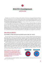
undesired thermal gradients between wafer center and edge (see Figure 3) eventually resulting in non-uniform
electrical and optical properties in solar cell structures.
FiguRE 3. Bowing of a wafer in the wafer carrier’s
pocket can lead to loss of thermal contact of the
wafer with the heated graphite (see fgure above for
convex and concave bow). This leads to undesired
thermal non-uniformity on the wafer surface causing T center
materials (fgure bottom)
In order to apply strain engineering without compromising the wafer yield a new design of the MOCVD reactor
growth chamber was needed.
13