Page 18 - RSE - Results of the Apollon Project
P. 18
Results of the APolloN PRoject ANd coNceNtRAtiNg PhotovoltAic PeRsPective
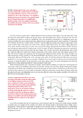
FiguRE 8. Temperature in the center and edge of
the wafer along with curvature behavior during the
experiment described in the text. The curvature is
measured in the center of the wafer. It is possible to
distinguish 4 zones: 1) Growth of the strained InGaP
layer, 2) Growth interruption and stabilization,
3) First variation of the H /N mixture underneath
2 2
the satellite, 4) Second variation of the H /N mixture
2 2
underneath the satellite
Once the InGaP was grown with a slightly different lattice parameter with respect to Ge, the wafer bent. After
observing the initial wafer bending, the growth process was interrupted and a proper amount of time was left
for allowing the system to reach its equilibrium. After the deposition interruption, an equilibrium status was
reached, in which the stress induced by lattice mismatch was compensated by the wafer curvature. At this point
-1
the curvature reached the constant value of 500 km and the difference between the surface temperature of the
centre and the edge of the wafers was around 20°C. Owing to wafer deformation, the surface edge temperature
of the wafer decreased with respect to the center (concave bending). Subsequently two different H2/N2 mixtures
were introduced underneath the satellite (zone 3 and 4 of Figure 9), while continuing measuring the evolution of
wafers temperatures and curvature. After the frst change, the curvature increased, till reaching the value of 800
-1
km , while the difference between the surface temperature of the centre and the edge of the wafers reached 30°C;
with the second change, the curvature and the temperature differences were zeroed. The results indicates the
high temperature tuning capability of the APOLLON MOCVD new heating system, since it is possible to eliminate
temperature differences between the center and edge of the wafer of even 30°C and make “fat” wafers presenting
defection of 1 mm (corresponding to a curvature of 800 km on a 4 inch wafer). It has also been proved that the
-1
presence of thermal gradient on the back side of the wafer allows control of wafer deformation and therefore
application of strain engineering without compromising the wafer yield.
When InGaP/InGaAs/Ge solar structures are grown, several switches between As-based and P-based gasses are
necessary to deposit the different semiconductor materials. During such switching, abrupt temperature changes
commonly occur, which make it diffcult to control the properties of such interfaces. Furthermore, if the total carrier
gas fow is kept constant, it is not possible to maintain a uniform temperature on deposition of both arsenide and
phosphide materials. Such diffculties have been overcome with the temperature tuning capability of the APOLLON
MOCVD reactor (see fgure 9 and 10).
FiguRE 9. Temperature behavior in the center
and edge of the wafer during the buffer growth
of two different triple junction runs: TJ 248
with no temperature profle tuning optimization,
TJ 251 with temperature profle tuning optimized.
Temperature profle tuning allows a fast
temperature control at the interface between
arsenide and phosphide materials, so that it
is possible to eliminate temperature spike at
interfaces; furthermore, by applying temperature
tuning it is possible to get uniform temperature
distribution both in arsenide and phosphide
materials
It is worth mentioning that the fast temperature control obtained with the temperature profle tuning capability
is possible since it is applied at the satellite level, where the thermal inertia is drastically reduced, while such a
temperature control would be impossible if applied at the susceptor level, as usually happens in conventional
MOCVD reactors; in this case, indeed, the greater material‘s mass would imply a too high thermal inertia for a fast
temperature control.
17