Page 19 - RSE - Results of the Apollon Project
P. 19
Results of the APolloN PRoject ANd coNceNtRAtiNg PhotovoltAic PeRsPective
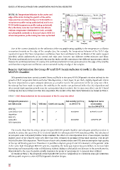
FiguRE 10. Temperature behavior in the center and
edge of the wafer during the growth of the entire
triple junction structure during run TJ 241 (with no
temperature profle tuning optimization) and in run
TJ 251 (with temperature profle tuning optimized).
The refectivity curve for run TJ251 is also shown.
Uniform temperature distribution in both arsenide
and phosphide materials is obtained only in RUN 251
where temperature profle tuning has been optimized
One of the current drawbacks in the utilization of the new profle tuning capability is the temperature oscillation
encountered mainly on the edge of the samples (see, for example, the temperature behavior of the TJ-251 edge
reported in Figure 10). These temperature oscillations have been attributed to the oscillation of the wafer support
(satellite), which underneath, in its central and edge zone, features two different H2/N2 mixtures and fows.
Therefore underneath in its central and edge zone the wafer satellite experiences two different gas pressures, which
induces its oscillatory behavior. Of course, this oscillatory behavior is more pronounced on the edge of the satellite
and therefore temperature oscillations are encountered mainly on edge of the samples.
Reactor Optimization for group-iv and iii-v Semiconductor growth in the Same
MOCvd Chamber
SiGe growths have been carried out with Silane and IBuGe in the same APOLLON growth chamber utilized for the
growth of III-V compounds. Before and after SiGe deposition, a GaAs layer, 10 µm thick, slightly doped with silicon
has been deposited on a GaAs undoped substrate, as a marker run for the assessment of the Ge carry over effect.
No attempt has been made to optimize the mobility in the marker run performed before the SiGe deposition and
after several triple junction growth runs. As a precaution taken to reduce the Ge carry over effect, one III-V-based
coating run has been carried out after SiGe deposition. The results of the Hall characterization are shown in Table 1.
tABLE 1. Hall characterization for the assessment of the Ge carry over effect
RUN/growth parameters Hall mobility (cm /V s) Background carrier
2
and Hall results T(°C) V/III ratio Growth rate (µm/h) at 300 K/77 K concentration
(cm ) at 300 K/77 K
-3
RUN 263,
16
GaAs before SiGe 650 21 7 4187/5492 8.9*10 / 7.6 10 16
deposition
RUN 279,
17
GaAs after 650 21 7 2631/2565 4.6*10 /5 10 17
SiGe deposition
The results show that by using a proper designed MOCVD growth chamber and adequate growth procedure is
possible to reduce the carry-over of Ge to a level suitable for subsequent III-V N-P junction growth. The selection of
an adequate solar cell polarity further helps minimize the effect of Ge incorporation in III-V based layers. Another
indirect proof of the reduced carry over effect has been obtained by growing several triple junction cells InGaP/
InGaAs/Ge after SiGe deposition. The fll factor of such cells showed values over 87% demonstrating the high quality
of the top cell limiting junction. Therefore it is possible to deposit group IV and III-V elements of the periodic table
in the same high throughput MOCVD systems, expanding the band gap engineering possibilities to increase light
harvesting and consequently solar cell effciency, without adding a substantial cost increase to the growth process,
which would be the case if separate growth chambers for group IV and groups III-V elements were utilized.
As shown in Table 2, the drawback of this new MOCVD reactor confguration is a relatively lower gas utilization
effciency with respect to other AIXTRON growth chamber designs.
18