Page 31 - RSE - Results of the Apollon Project
P. 31
29 Results of the APOLLON project and Concentrating Photovoltaic perspective
epitaxial processes is mandatory to reduce the defects in the epitaxial materials. In APOLLON two different routes
have been investigated:
• MOCVD growth by using new precursors for Ge and Si
• low-energy plasma-enhanced chemical vapour deposition (LEPECVD)
The first route has been followed by CNRS. Preliminary tests of Si epitaxy have been performed by using
TrichloroSilane (TCS). Superlattices [Ge/Si] x 4 on GaAs (100) substrates and on Ge (100) 6°off with TCS and IBuGe as
precursors have been grown and characterized. 1.9 nm thick strained Si layers have been obtained embedded in Ge
RESuLtS OF thE APOLLON PROjECt ANd CONCENtRAtiNg PhOtOvOLtAiC PERSPECtivE
with high quality (see Figure 23). Unfortunately high growth temperature values > 725C°C were necessary to obtain
good morphologies, therefore this route was not further implemented in the project. Furthermore, CNRS found it
difficult to produce SiGe buffer layer with reproducible Ge concentration in the epilayers. Different precursors
should be experimented for the realization of SiGe virtual substrate by MOCVD.
FiguRE 23. TEM cross-section of Ge/Se superlattices grown on GaAs ( left) and Ge ( right) substrates
Figure 23. TEM cross-section of Ge/Se superlatteces grown on GaAs ( left) and Ge ( right) substrates
The University of Ferrara has investigated the production of SiGe buffer layers by means of Low Energy
PECVD (LEPECVD) trying to produce Ge layers with surface threading dislocation density compatible with the
The University of Ferrara has investigated the realization of SiGe buffer layers by of Low Energy PECVD (LEPECVD)
heteroepitaxial of III-V triple junction solar cells. The main driver for this research was the achievement of SiGe
trying to produce Ge layers with surface threading dislocation density compatible with the heteropitaxial of III-V
6
-2
virtual substrates with surface threading dislocations density (TDD) down to a value lower than 10 cm , in order
triple junction solar cells. The main driver for this research was the achievement of SiGe virtual substrates with
-2
6
to avoid the detrimental effects of crystal defects leading to minority carrier recombination. In the framework of
surface threading dislocations density (TDD) down to a value lower than 10 cm , in order to avoid the detrimental
2
5
the project it was possible to obtain SiGe virtual substrates having a dislocation density in the range of 5x10 cm- ,
effects of crystal defects leading to minority carrier recombination. In the framework of the project it was possible to
in agreement with the target of the project, as revealed from the etch pit density count (see Figure 24), however the
2
5
realize SiGe virtual substrates having a dislocation density in the range of 5x10 cm- , in agreement with the target of
typical residual surface roughness was in the range of 50-90 nm RMS, thus regarded as too high to get epi layers with
the project, as revealed from the etch pit density count (see
mirror like morphologies.
Figure 24), however the typical residual surface roughness was in the range of 50-90 nm RMS, and it was judged too
30 Results of the APOLLON project and Concentrating Photovoltaic perspective
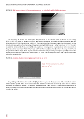
FiguRE 24. Scanning electron microscope etch pit count on Ge on Si
high to get epilayers with mirror like morphologies.
Wafer 170 (thickness capping Ge = 1.5 μm)
5 -2
EPD = 3.2 · 10 cm
Figure 24. Scanning electron microscope etch pit count on Ge on Si.
Pre-polishing of the SiGe wafers has been highlighted as a key step in the preparation of the virtual SiGe wafers
before epitaxial growth. It has been discovered that in order to obtain mirror like III-V epi layers over SiGe virtual
Pre-polishing of the SiGe wafers has been evidenced as a key step in the preparation of the virtual SiGe wafers prior
substrates, in addition to the low TTD required, suffciently thick (5µm) capping Ge layers are required over Si, in
of epitaxial growth. It has been discovered that in order to obtain mirror like III-V epilayers over SiGe virtual
order to properly accomplish the polishing step and get a roughness that is as comparable as possible with that of
substrates, apart the required low TTD, enough thick (5µm) capping Ge layers are required over Si, in order to
accomplish properly the polishing step and get a roughness as much as possible comparable with that of standard Ge
standard Ge wafers.
wafers.
30
epitaxial processes is mandatory to reduce the defects in the epitaxial materials. In APOLLON two different routes
have been investigated:
• MOCVD growth by using new precursors for Ge and Si
• low-energy plasma-enhanced chemical vapour deposition (LEPECVD)
The first route has been followed by CNRS. Preliminary tests of Si epitaxy have been performed by using
TrichloroSilane (TCS). Superlattices [Ge/Si] x 4 on GaAs (100) substrates and on Ge (100) 6°off with TCS and IBuGe as
precursors have been grown and characterized. 1.9 nm thick strained Si layers have been obtained embedded in Ge
RESuLtS OF thE APOLLON PROjECt ANd CONCENtRAtiNg PhOtOvOLtAiC PERSPECtivE
with high quality (see Figure 23). Unfortunately high growth temperature values > 725C°C were necessary to obtain
good morphologies, therefore this route was not further implemented in the project. Furthermore, CNRS found it
difficult to produce SiGe buffer layer with reproducible Ge concentration in the epilayers. Different precursors
should be experimented for the realization of SiGe virtual substrate by MOCVD.
FiguRE 23. TEM cross-section of Ge/Se superlattices grown on GaAs ( left) and Ge ( right) substrates
Figure 23. TEM cross-section of Ge/Se superlatteces grown on GaAs ( left) and Ge ( right) substrates
The University of Ferrara has investigated the production of SiGe buffer layers by means of Low Energy
PECVD (LEPECVD) trying to produce Ge layers with surface threading dislocation density compatible with the
The University of Ferrara has investigated the realization of SiGe buffer layers by of Low Energy PECVD (LEPECVD)
heteroepitaxial of III-V triple junction solar cells. The main driver for this research was the achievement of SiGe
trying to produce Ge layers with surface threading dislocation density compatible with the heteropitaxial of III-V
6
-2
virtual substrates with surface threading dislocations density (TDD) down to a value lower than 10 cm , in order
triple junction solar cells. The main driver for this research was the achievement of SiGe virtual substrates with
-2
6
to avoid the detrimental effects of crystal defects leading to minority carrier recombination. In the framework of
surface threading dislocations density (TDD) down to a value lower than 10 cm , in order to avoid the detrimental
2
5
the project it was possible to obtain SiGe virtual substrates having a dislocation density in the range of 5x10 cm- ,
effects of crystal defects leading to minority carrier recombination. In the framework of the project it was possible to
in agreement with the target of the project, as revealed from the etch pit density count (see Figure 24), however the
2
5
realize SiGe virtual substrates having a dislocation density in the range of 5x10 cm- , in agreement with the target of
typical residual surface roughness was in the range of 50-90 nm RMS, thus regarded as too high to get epi layers with
the project, as revealed from the etch pit density count (see
mirror like morphologies.
Figure 24), however the typical residual surface roughness was in the range of 50-90 nm RMS, and it was judged too
30 Results of the APOLLON project and Concentrating Photovoltaic perspective
FiguRE 24. Scanning electron microscope etch pit count on Ge on Si
high to get epilayers with mirror like morphologies.
Wafer 170 (thickness capping Ge = 1.5 μm)
5 -2
EPD = 3.2 · 10 cm
Figure 24. Scanning electron microscope etch pit count on Ge on Si.
Pre-polishing of the SiGe wafers has been highlighted as a key step in the preparation of the virtual SiGe wafers
before epitaxial growth. It has been discovered that in order to obtain mirror like III-V epi layers over SiGe virtual
Pre-polishing of the SiGe wafers has been evidenced as a key step in the preparation of the virtual SiGe wafers prior
substrates, in addition to the low TTD required, suffciently thick (5µm) capping Ge layers are required over Si, in
of epitaxial growth. It has been discovered that in order to obtain mirror like III-V epilayers over SiGe virtual
order to properly accomplish the polishing step and get a roughness that is as comparable as possible with that of
substrates, apart the required low TTD, enough thick (5µm) capping Ge layers are required over Si, in order to
accomplish properly the polishing step and get a roughness as much as possible comparable with that of standard Ge
standard Ge wafers.
wafers.
30