Page 30 - RSE - Results of the Apollon Project
P. 30
Results of the APolloN PRoject ANd coNceNtRAtiNg PhotovoltAic PeRsPective
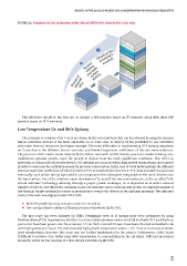
FiguRE 22. Sequence for the realization of the bifacial (BFC) SiGe-GaAs-InGaP solar cells
This MJ device would be the frst one to include a N/P junction based on IV elements along with other N/P
junction based on III-V elements.
Low temperature ge and Sige Epitaxy
The attempts to combine of III-V on Si are driven by the cost reduction that can be achieved by using the cheaper
silicon substrates instead of the more expensive Ge or GaAs ones, as well as by the possibility to use substrates
with lower thermal resistance and higher strength. The main diffculties in implementing III-V epitaxy deposition
on Si are due to the different lattice constants and thermal expansion coeffcients of the two semiconductors.
The presence of the elastic strain induced by the lattice mismatch and the kinetic processes involved during non-
equilibrium epitaxial growth, cause the growth to deviate from the ideal equilibrium conditions. This effect, in
particular, is enhanced in thermally driven CVD epitaxial processes, in which high growth temperatures are required
in order to overcome the activation energy for precursor dissociation. In the case of Ge/Si heteroepitaxy, the different
-1
thermal expansion coeffcients of Silicon (2.6x10⁻⁶ °C ) and Germanium (5.8 x10⁻⁶ °C ) cause the wafer to bend and
-1
eventually crack within the epi layer, which can compromise the subsequent overgrowth of electronic devices onto
the layer surface. One of the solutions under development “to match” the two semiconductors, is the so called “SiGe
virtual substrate” technology, whereby, through a proper growth technique, Ge is deposited on Si with a reduced
number of defects, over which the remaining solar cell structure can be subsequently grown. The implementation of
low thermal-budget epitaxial processes is mandatory to reduce the defects in the epitaxial materials. Two different
routes have been investigated under APOLLON:
p MOCVD growth by using new precursors for Ge and Si;
p low-energy plasma-enhanced chemical vapour deposition (LEPECVD).
The frst route has been followed by CNRS. Preliminary tests of Si epitaxy have been performed by using
TrichloroSilane (TCS). Superlattices [Ge/Si] x 4 on GaAs (100) substrates and on Ge (100) 6°off with TCS and IBuGe as
precursors have been grown and characterized. 1.9 nm thick strained Si layers have been obtained embedded in Ge
with high quality (see Figure 23). Unfortunately high growth temperature values > 725 °C were necessary to obtain
good morphologies, therefore this route was not further implemented in the project. Furthermore, CNRS found
it diffcult to produce SiGe buffer layer with reproducible Ge concentration in the epi layers. Different precursors
should be tested for the creation of a SiGe virtual substrate by MOCVD.
29