Page 41 - RSE - Results of the Apollon Project
P. 41
Results of the APolloN PRoject ANd coNceNtRAtiNg PhotovoltAic PeRsPective
form, and then chemically etched as is normally done for the assembly of PCB.
Due to the way the substrate is made, high thicknesses of conductor materials can be achieved, thus substrate
size can be reduced.
The copper is usually bonded on both sides, allowing a better thermal exchange with the heat-sink. The surface
fnishing of the copper can be as the standard one used for the PCB industry, so it can be bondable or solderable.
4. THICK FILM ON ALUMINIUM
Thick flm process can also be adopted on an aluminum substrate, but FiguRE 39. Thick flm on aluminium
an insulating layer is necessary to insulate the conductor tracks to the
conductor substrate.
The circuit traces are screen printed onto an aluminum layer, which
could also act a heat sink for itself. The thickness of the insulating layer
ranges between 60-70μm, for 1000V insulation, while the conductor layer
thickness is 150-180μm.
The main advantage of this solution is its thermal performance, but due
to the low breakdown voltage, this solution is not considered suitable for
PV application.
After an evaluation of all possible substrates, thick flm on ceramic substrates (Al O ) has been selected for the
2 3
APOLLON project for the following reasons: IMS has a low thermal performances, thick flm on aluminium has a low
breakdown voltage and the DCB substrate is too expensive for the PV concentration application.
Receivers Fabrication
After substrate selection, CRP designed and developed second generation solar receivers based on thick flm
on alumina (Al O ) substrates by chip-on-board technology. The assembly is made of three steps: die attach, wire
2 3
bonding and SMT (Surface Mounted Technology) assembly.
DIE ATTACH
Chip attachment is the frst process in die assembly. The chip is adhered to the die pad on the board, after which
wire bonding is done using a wedge or ball bonder. One of the challenges of COB package technology is the bare
chip placement. The need is to assemble complex devices at high speeds, with high consistency, and at low costs.
Accurate placement of the bare die on the substrate with ever fner pitch and denser routing layouts is necessary.
For wire bonded COB, inaccurate chip placement may cause insuffcient adhesive coverage around the die and
therefore imperfect die attach which causes yield problems.
For the assembly of the solar receivers the dot dispense method has been used, using epoxy silver flled adhesive.
The dispensing patterning and the process parameters have been optimized in order to guarantee a good adhesion
between cell and substrates avoiding air void that can induce cell breakdown. The monitoring of the process
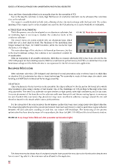
optimization has been done by means of x-ray analysis, die shear test (MIL STD-883) and electrical characterization.
FiguRE 40. X ray image before (left) and after parameter optimization (right)
Die shear test results shows that all analyzed samples have passed the test, due to the fact that the detachment
force is over 5 kg, which is the minimum value allowed in the regulation.
40