Page 42 - RSE - Results of the Apollon Project
P. 42
Results of the APolloN PRoject ANd coNceNtRAtiNg PhotovoltAic PeRsPective
FiguRE 41. Die shear test operation condition and test results
Number of test 5
Medium breaking force 14,9 kg
Standard deviation 9,2 kg
Successful 5
Not successful 0
WIRE BONDING
Die attach is followed by thermo-compression of gold wire, bonding each chip bond pad to the corresponding
bond pad on the PCB. Wire bonding is the most widely used technique for electrical chip interconnections in the
microelectronics industry. Figure 42 shows schematically a wire bonding chip on board and a mounted cell on
substrate.
FiguRE 42. Wire bonding scheme (left) and Ceramic substrate after wire bonding (right)
The wire bonding process parameters optimization has been carried out and the cell has been tested by wire pull
test (MIL STD-883) in order to assess the quality of the bondings. Wire pull test results show (see Figure 43) all the
analyzed samples have passed the test, due to the fact that the breaking force is over 7 g, which is the minimum
value allowed in the regulation.
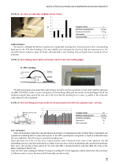
FiguRE 43. Wire Pull Testing and some results (all the measurement are above the regulation limit – red line)
Number of test 20
Medium breaking force 25,4 kg
Standard deviation 3,5 kg
Successful 20
Not successful 0
SMT ASSEMBLy
After cell assembly, connectors and the bypass diode have to be integrated in the receiver. These components are
suitable for soldering with Sn alloy solder paste. In the SMT assembly the component is made of solderable leads
that are soldered to the PCB using a conventional refow oven.
Figure 44 shows one of the receivers thus created, with the solar cell placed in the center of the substrate. The full
assembling process is has been performed as a large scale one, since even at prototyping scale, production machines
were used. The receiver is then placed on the heat sink with a thermal interface material, with the focus of the
mirror pointing at the PV cell.
Solar receivers have undergone lifetime testing of according IEC 62108 regulation, which determines the procedure
to follow in order to stress the device both thermally and electrically.
41